Activity 5: Multiple scattering in the forward scattering regime#
In photoelectron diffraction, it is well known that for high photoelectron kinetic energy (typically > 900 eV), the scattering factor is strongly peaked in the forward direction. It means that photoelectrons are almost not deviated after a scattering event.
Peaks of intentisity are then usually observed for dense atomic directions of the sample. This is the forward scattering approximation.
For such high kinetic energy, multiple scattering is needed to accurately describe the measured intensity, but the matrix inversion algorithm cannot be used since the memory needed for storing the matrix itself would be generally too large. The matrix will contain \((N \times (L_{max}+1)^2)^2\) elements of complex type with double precision (64 bits) where \(N\) is the number of atoms and \(L_{max}\) is the number of spherical harmonics used to expand the electron wave around each atomic center. As the kinetic energy increases, the mean free path (MFP) of the photoelectron is larger and the number of atoms in the cluster has to be greater. Lmax also increases with the kinetic energy.
Try to evaluate how much memory you would need for this matrix for a hemispherical cluster of copper 15 angströms thick (1 MFP) for \(L_{max} = 25\) ?
Show code cell content
import numpy as np

# lattice constant of fcc copper
a = 3.6
# radius of the cluster
r = 15
# volume of the cluster
V = .5 * (4/3) * np.pi * r**3
# volume of the cell
v = a**3
# number of atoms in the unit cell
n = 4
# number of atoms in the cluster
N = int(V/v * n)

Lmax = 25
M = (N * (Lmax+1)**2 )**2 * 2 * 64 / 8
print(f"{N:d} atoms, {M/1e12:.3f} TB")
606 atoms, 2.685 TB
This is too much memory. We will use another algorithm available in MsSpec: The Rehr-Albers series expansion. We already used that algorithm in activity 3 for the single scattering approach. But this time, we will explore a bit more the effect of the scattering order > 1
PED of the 1T-TiSe2 surface#
Let us try to model the Ti2p XPD pattern of the transition metal dichalcogenide 1T-TiSe2.
See also
based on this paper from M.V. Kuznetsov et al. Surf. Sci. 606 p1760–70 (2012)
Creating the TiSe2 cluster#
Start by creating a small cluster of 1T-TiSe2 using the mx2 function of ase.build and the hemispherical_cluster function of msspec.utils.
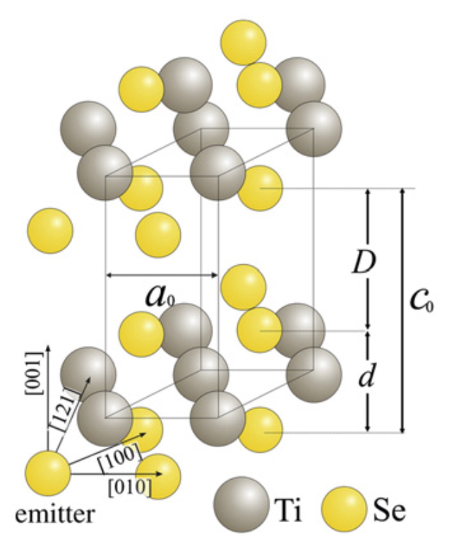
Fig. 11 Structure of 1T-TiSe2 (\(a_0=b_0=3.535\) Å, \(c_0=6.004\) Å, \(d=3.450\) Å, \(D=2.554\) Å)#
Complete the code snipet provided below to create a small TiSe2 cluster with Ti emitter in the 2nd plane:
 1from ase.build import mx2
 2from ase.visualize import view
 3from msspec.calculator import MSSPEC
 4from msspec.utils import hemispherical_cluster, get_atom_index
 5
 6# Some usefull constants (a, c, d, D) for defining the structure
 7a=...
 8
 9# Create the TiSe2 trilayer
10# use ase help for this function
11TiSe2 = mx2(formula=...)
12
13# The preious cell is 2D, let's define the c-axis to take into account
14# the Van der Waals gap between trilayers
15TiSe2.cell[2] = [0, 0, ...]
16
17# To be aligned like in the paper
18TiSe2.rotate(60, 'z', rotate_cell=True)
19
20# Since the material is multi-elements, "tag" each inequivalent atom
21# of the unit cell with a number. The "Ti" atom is tagged 0 and "Se"
22# atoms are 1 and 2.
23for i in range(3):
24    TiSe2[i].tag = i
25
26cluster = hemispherical_cluster(TiSe2, emitter_tag=..., emitter_plane=..., planes=5)
27cluster.emitter = get_atom_index(cluster, 0, 0, 0)
28
29view(cluster)
30
Show code cell content
from ase.build import mx2
from ase.visualize import view
from msspec.calculator import MSSPEC
from msspec.utils import hemispherical_cluster, get_atom_index

# Some usefull constants (a, c, d, D) for defining the structure
a=3.535;c=6.004;d=3.450;D=2.554

# Create the TiSe2 trilayer
# use ase help for this function
TiSe2 = mx2(formula='TiSe2', kind='1T', a=a, thickness=d, size=(1, 1, 1), vacuum=None)

# The preious cell is 2D, let's define the c-axis to take into account
# the Van der Waals gap between trilayers
TiSe2.cell[2] = [0, 0, c]

# To be aligned like in the paper
TiSe2.rotate(60, 'z', rotate_cell=True)

# Since the material is multi-elements, "tag" each inequivalent atom
# of the unit cell with a number. The "Ti" atom is tagged 0 and "Se"
# atoms are 1 and 2.
for i in range(3):
    TiSe2[i].tag = i

cluster = hemispherical_cluster(TiSe2, emitter_tag=0, emitter_plane=1, planes=5)
cluster.emitter = get_atom_index(cluster, 0, 0, 0)
Effect of the scattering order#
Use the line belows to create a calculator and compute a \(\theta\)-\(\phi\) scan of the Ti(2p)
# Create a calculator with Rehr-Albers series expansion algorithm
calc = MSSPEC(spectroscopy='PED', algorithm='expansion')
calc.set_atoms(cluster)

data = None
for ndif in range(1,4):
    calc.calculation_parameters.scattering_order = ndif
    data = calc.get_theta_phi_scan(level='2p', kinetic_energy=1030, data=data)

data.view()
Compute a scan for an emitter in the first trilayer and in the second trilayer for scattering orders from 1 (single scattering) to 3 in order to complete the figure below.
What do you conclude about the value of the calc.calculation_parameters.scattering_order ?
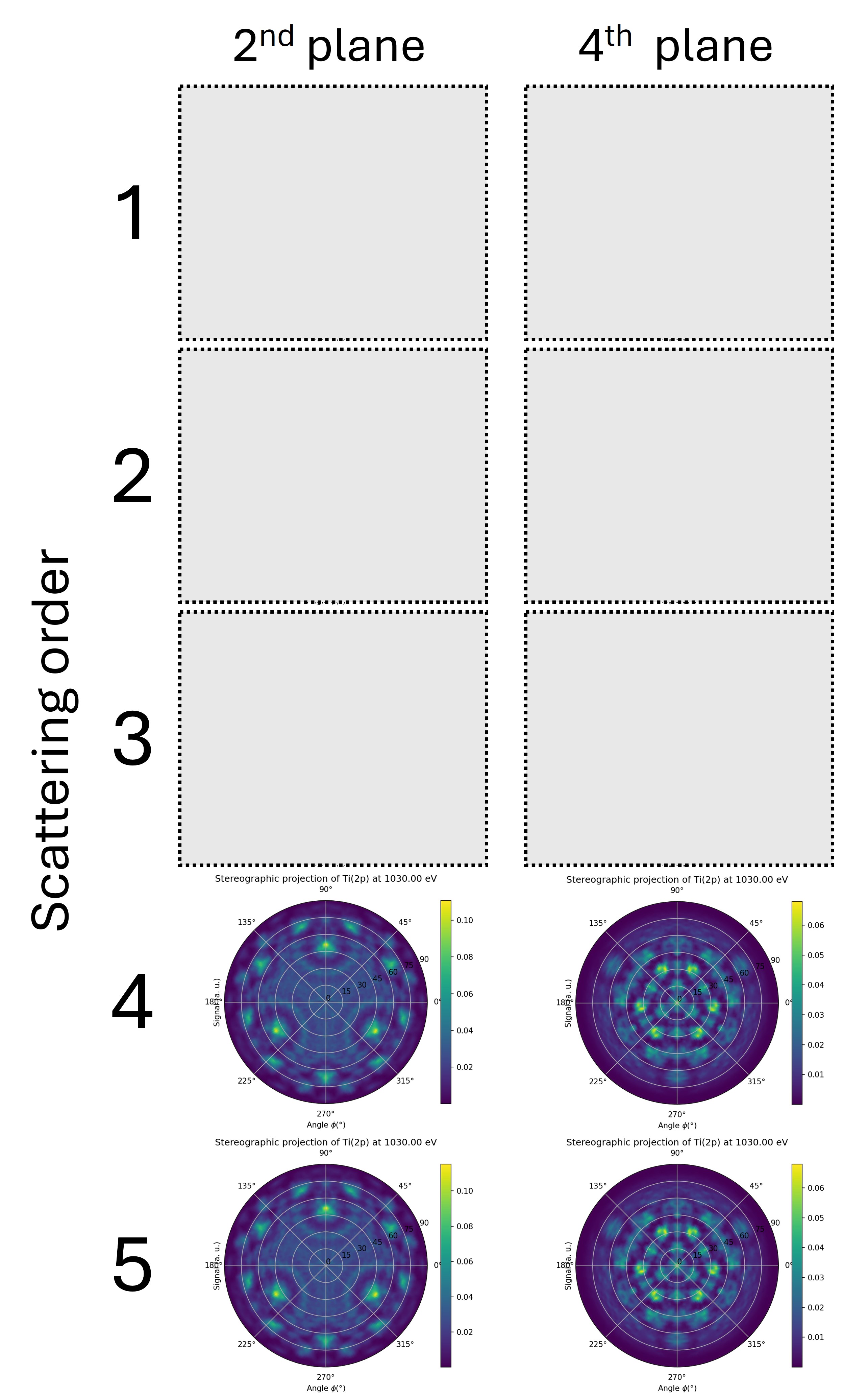
Fig. 12 \(\theta\)-\(\phi\) scan of Ti(2p) at 1030 eV kinetic energy for an emitter in the first trilayer (left column) and in the second trilayer (right column). Each row correspond to a growing value for the calc.calculation_parameters.scattering_order parameter (from 1 to 5).#
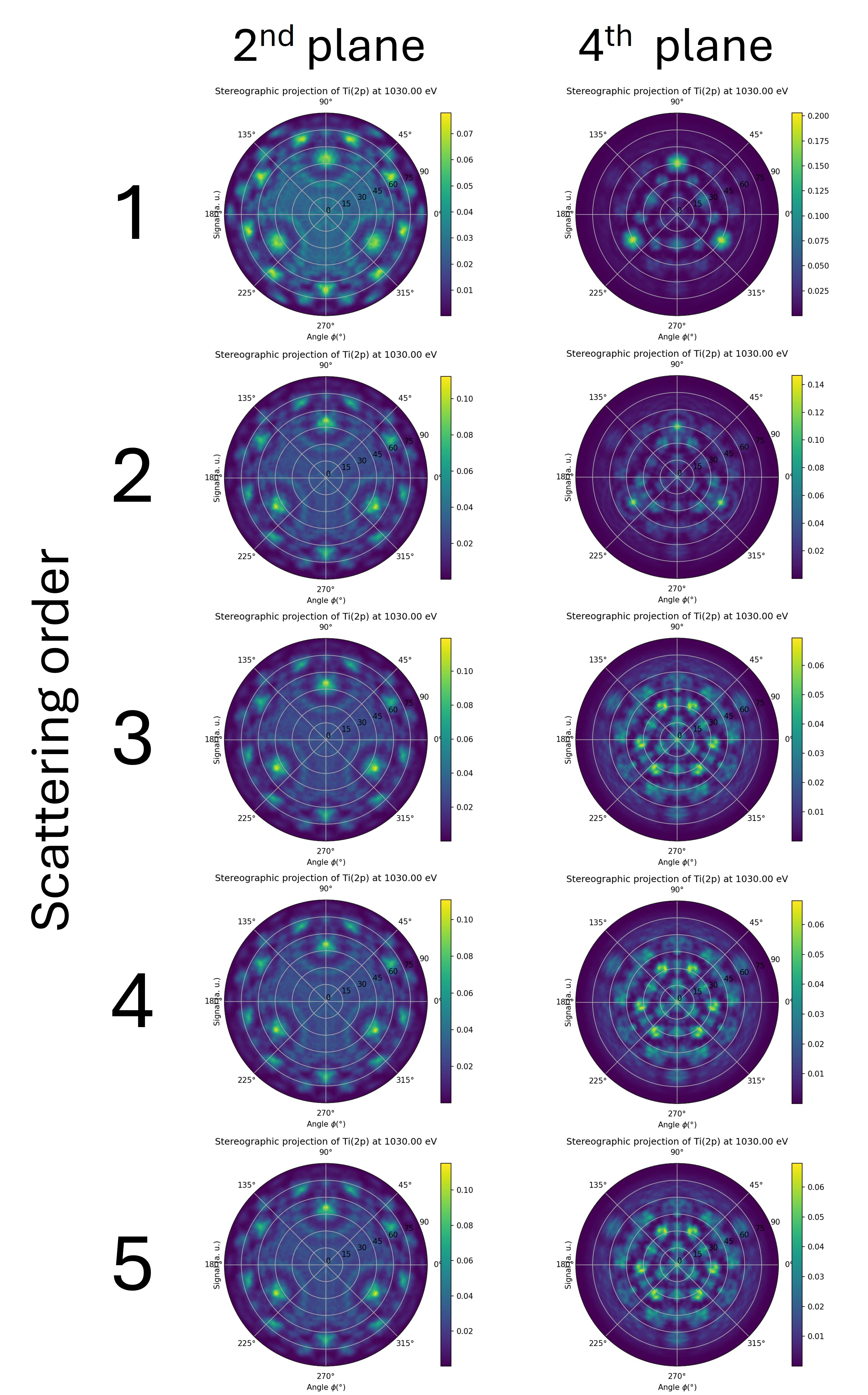
Fig. 13 \(\theta\)-\(\phi\) scan of Ti(2p) at 1030 eV kinetic energy for an emitter in the first trilayer (left column) and in the second trilayer (right column). Each row correspond to a growing value for the calc.calculation_parameters.scattering_order parameter (from 1 to 5).#
The deeper the emitter, the greater the scattering order should be for the intensity to converge. Typically, in the forward scattering regime, the scattering order corresponds to the number of planes above the emitter.